Generating or using a reset signal

What’s the recommended way to generate a reliable RST signal to the modules? It doesn’t look as if you have a dedicated micro-to-FPGA line to send a reset (and that could be prone to race conditions anyhow during configuration).

I suppose that doing a small soft-reset module would probably be preferable. Use a few bits worth of register as a counter (depending on the fact that the FPGA uses global-reset to force all of the flops to 0), and generate RST or /RST until counter clock-counts up to its maximum value?

Or, if one is using one or more PLLs, assert RST until all of the PLLs report lock?

Or both of the above (use a counter, but don’t start counting until the PLLs are locked)?

Fun stuff… I just coded up a little I2S transmitter from scratch, got it working in iverilog, and now need to turn it into a real design with a real clock source and reset-initialization.

Dave,

There are many ways to implement a reset for the ShastaPlus FPGA module.

We started writing a blog to discuss the many ways to generate a reliable reset and the varying degrees of complexity. That blog was also talking about asynchronous signals so that started a different thread into that matter. We should get those blog postings up shortly.

To address your need and likely others very soon we do have a module to use to generate an internal reset signal.

The fact, as you as well stated, the FPGA due to its nature, handles the critical post power on initialization. We can use that fact to create a simplified power on reset signal for use within our digital logic designs. The FPGA synchronously clears all flops during initialization. Initialization can’t occur until the power supplies are stable and its internal generated clock is stable.

Our external clock source, as well as the HS_OSC will also be stable by the time initialization is complete. The internal PLL will produce a lock state status bit, which can be used if the PLL is in a time critical path.

The module below produces a reset pulse to be used in your always blocks that need a reset state.

//////////////////////////////////////////////////////////////////////
//
// WF_reset
//
// General reset circuit
// Will detect FPGA just loaded and produce a reset pulse
// for all synchronous logic to be reset
//
// outputs a 1 clock pulse when after FPGA is loaded indicating reset.
//
// instantiation example:
//
// WF_reset my_reset (
// .clk(clk), // clock domain which reset is valid
// .reset_out(myreset));
//
///////////////////////////////////////////////////////////////////////

module WF_reset (
input wire clk, // clock
output wire reset_out // 1 clk pulse for reset
);

 reg  [1:0] resets;

 always @ (posedge clk)
   if (resets == 2'b0)     // just came out of reset
     resets <= 2'b01;
   else
     resets <= {resets[0],resets[1]};   // rotate  - stops optimization of signal

assign reset_out = (resets == 2’b0);

endmodule
/////////////////////////////////////////////////////////////////////////////////////////

This above doesn’t require an external pin.
Other methods are possible for a power on reset and the blog will go in more detail.
The above method should get you started, especially if you need to initialize state bits to a non zero values.

For simulation with iverilog the fact that a FPGA is initialized is not know to iverilog. iverilog, as with most simulators, starts the state info as “x” or unknown. Having an external reset typically solves the “x” issues. To use the internal reset module with a logic simulator it is necessary to initialize some state info into known states so the simulation doesn’t diverge into all “x” states.

Using the force and release selectively will resolve this problem.
I am not sure how far you are in simulating your design but I can help you initialize the above module to allow simulations to run.

If you want to use a external reset you can add an external circuit or use the MCU to generate a reset signal which can be controlled via the web page, java, or phython.

I prefer the internal reset method, since it is self contained. Granted if using the FPGA module as one part in a larger design, some sort of system power on reset (POR) must be used.

MIck

Hi, Mick! Thanks for the information and suggestions.

I made a good deal of progress along these lines over the past week. After doing some reading I came to the same conclusions you suggest: a simple internal reset based on a counter would work and be reliable. I made one using a 4-bit counter, for a longer reset pulse (I figured I might want to wire it to a board pin to reset some external logic that might need a wide pulse). With that in the real design, and some of the usual initial-block-and-delay techiques for iverilog, I got the design to reset and wake up properly.

I’ve been throwing together what I hope will be a workable design for an FM-stereo test-signal generator, and the first part is working both in iverilog simulation and on the ShastaPlus using icestorm. I coded up an I2S transmitter (16-bit) and learned some things I shouldn’t do (don’t
try to control the flipflops using both positive- and negative-edge triggering; best to put all logic to control a reg within a single always block) and it now runs. I don’t have a DAC board hooked up to it yet, but the waveforms look good on my o’scope.

I added a low-distortion sinewave generator this weekend (used up 16 of the embedded block RAMs, and one DSP block to do some linear interpolation).

This is really great good fun! I’ve been doing embedded software for decades, and reading other peoples’ hardware designs, but I’ve never ventured into doing my own digital designs in an FPGA. Looking at the problem “sideways” (massively-parallel operation and explicit pipelines) rather than sequentially is a new experience and a bit of a mind-stretcher.

Dave,

Good to hear about a really fun and interesting project. Your are really utilizing the FPGA advance capabilities.

I need to publish a list of strongly recommended DO’s and DONTs for verilog coding to keep new comers out of trouble. It is always possible to use both edges but it does come with complications, and your point of a register assignments need to be in one always block.

Keep us posted on how the project is coming.

MIck

Hi, Mick! Good progress so far.

Goal: create an FM-stereo test generator which can output either a composite stereo-audio signal (the usual commercial-FM subcarrier system), or an I/Q quadrature signal that can drive the generation of a 10.7 MHz IF signal which is frequency-modulated by the composite signal. The D-to-A step will be done by a fairly standard audio DAC like the one you sell, drive by I2S at 192000 samples/second.

Steps needed: generate at least four sinewaves - L and R channel audio, 38 kHz subcarrier, and 19 kHz pilot signal. Perform matrixing (create L+R and L-R), multiply L-R by 38 kHz subcarrier (creating a double-sideband suppressed-carrier signal), mix this with L+R and with the pilot tone. The amplitude of this composite signal then controls the phase advance of two more sinewaves (in quadrature) which will be output to the DAC and I/Q mixers (the mixer LO will eventually be a quadrature pair of 10.7 MHz squarewaves from the FPGA).

Gain controls are needed on all inputs. All signals should be low-noise low-distortion (near-CD-quality - no less than 14 bits).

Mighty scary for a first FPGA project… the angels might decide not to tread here, but I have nothing to lose in trying.

Lots of math required - minimum of six sinewaves to compute/interpolate, mixing and multiplying to create the composite signal, and a dash of TPDF dither thrown in to keep the distortions down. A big Vertex 7 might be able to do this by brute force, but if I tried it in the ICE40 I’d run out of gates or timing pretty quickly.

Fortunately the timing requirements aren’t bad… the bit clock will be under 7 MHz, and there are 32 clocks between each new set of 16-bit samples being needed. Brute force isn’t required. I can break the problem up into three or four separate processing pipelines (sinewave phase-advance, sinewave lookup/interpolation, multiplex-mixing, and frequency modulation). Each pipeline needs just one multiply-and-accumulate resource and a bunch of multiplexing logic for the inputs and outputs. I think I have enough cycles to handle a dozen sinewave test signals, not just two.

So - what’s working? I2S transmitter came first… quite easy. The sinewave pipeline came second - this uses one MAC and 16 of the BRAMs to make a couple of big register arrays. I’m getting 15 bits or so of effective resolution out of it.

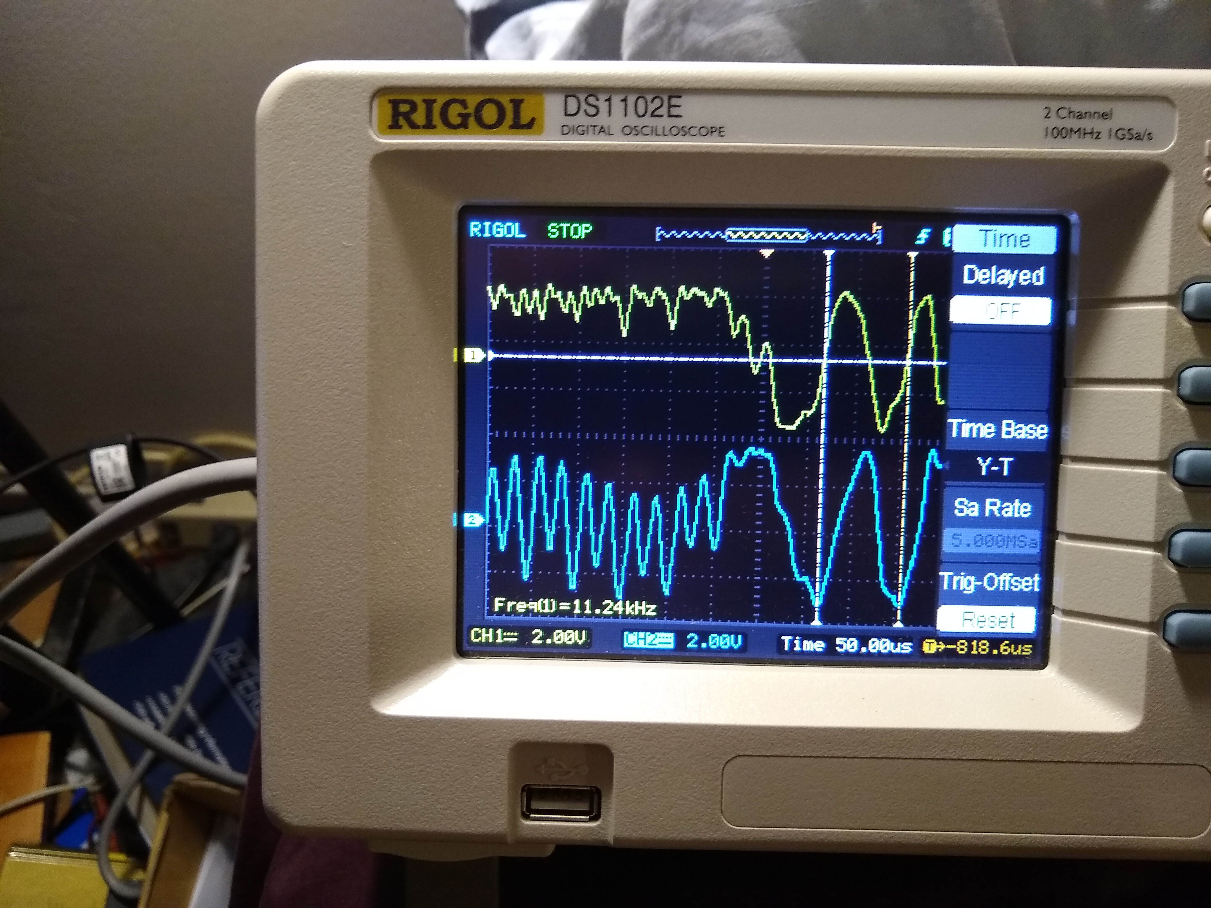
I wrote the stereo multiplexer/mixer this week, and got it working in behavioral Verilog under iverilog a couple of days ago. The results look quite good.

Getting things to synthesize under yosys was interesting. The design did build, but it was using more logic cells (29%) and fewer SB16_MACs (1) than I expected. I dug into the JSON and source code, and found that the current version of yosys will infer the use of the hardware MAC only for an unsigned multiply (not the addition, and not any signed operations).

So, I rewrote that one step of the sinewave and multiplexer pipelines to use explicitly instantiated SB_MAC16 blocks. Once I figured out what configurations I wanted (controls, and registration-or-not) the design started working again in iverilog… and it now synthesizes using two DSP blocks, and only 12% of the logic cells. Looks like plenty of resources left for other things (the frequency modulator and phase advance, controls, multiple operating modes, and so forth).

I need to wire up my DAC board and actually hook it up to the Shasta and confirm that it can run at speed.

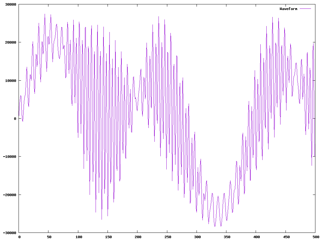
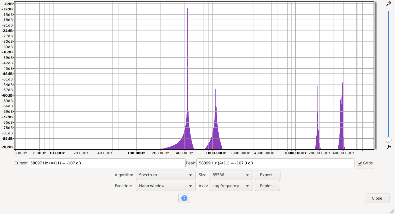
Attached is a plot of the composite-output signal (generated by iverilog $monitor) and an Audacity spectrum analysis. The test inputs are 440 and 1000 Hz audio signals (L and R).

fm 192k-tpdf

More good progress this week - I’ve got actual analog signals out.

I wrote the “amplitude to frequency modulation I/Q” block (pretty simple, needs one MAC16). Converted the test signal constants (e.g. frequency and amplitude) to programmable ones - one 256x16 block-ram currently holds four sets of test parameters, and pressing the button on the board rotates between them (I cribbed from your de-bouncing code). The outputs to I2S are now selectable: phase angle, sinewave, composite signal, or the I/Q modulator output.

The design currently takes 31% of the logic cells, and half of the BRAMs and DSPs.

I wired some pins onto the little PCM5102A board I had ebayed, installed some jumpers, and (after the usual troubleshooting) was off to the races.

Sinewaves:

Baseband_audio_signals

Composite audio below, and the subcarrier above for reference:

Composite_audio_and_subcarrier

Quadrature signals:

FM_I_and_Q

FM_I_vs_Q