FPGA 10kHz oscillator

Built-in Low Frequency Clock

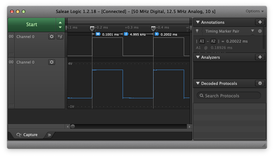
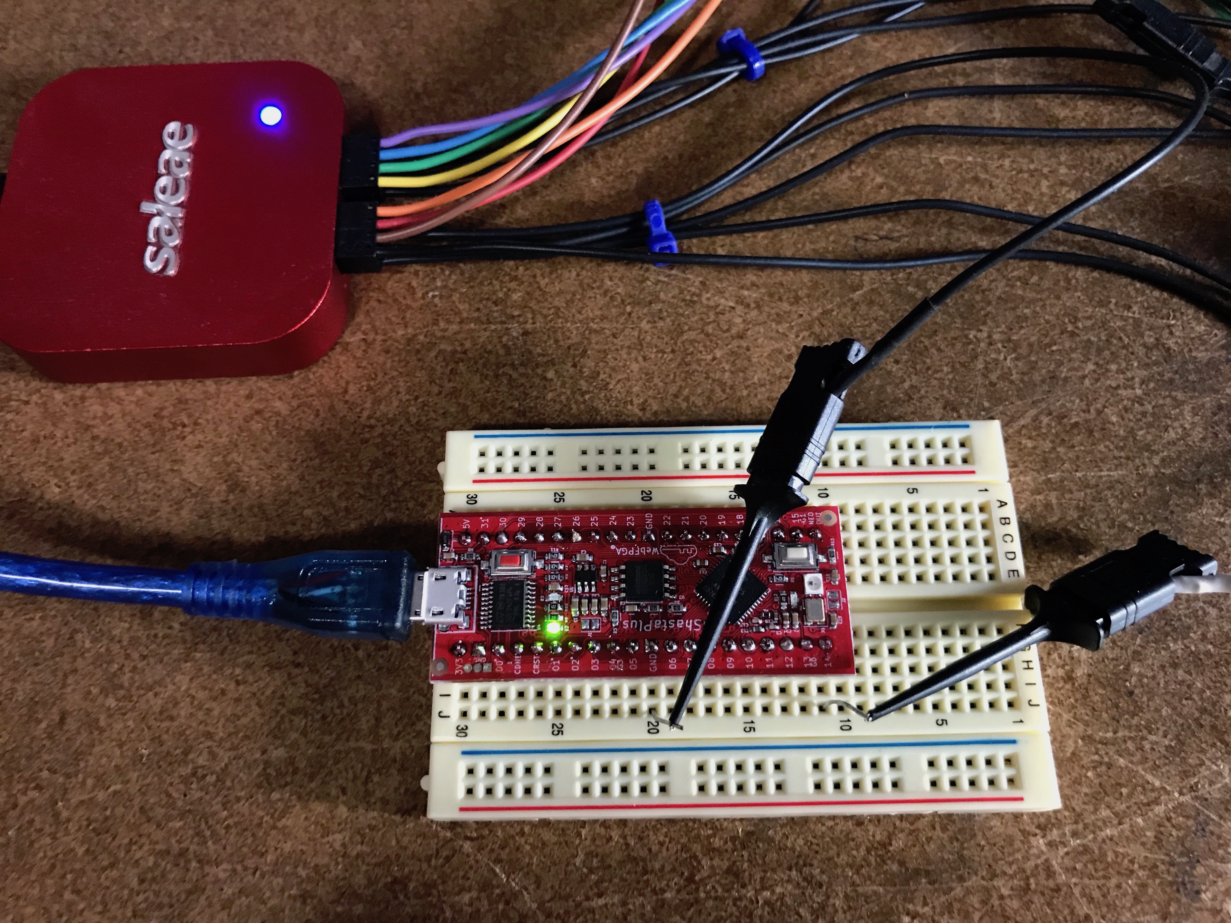
Here is one way to “see” the FPGA low frequency clock.

// ShastaPlus single pin toggle LF OSC, rr Oct 15, 2019
// PC board pin 14 to saleae; PC gnd to saleae gnd
// Pin 14 monitors one half of 10 kHz FPGA oscillator.

// @MAP_IO PIN_14 14

module fpga_top(output wire PIN_14);

reg [0:0] counter; reg state0;
assign PIN_14 = state0;

wire	clk_en = 'b1;
SB_LFOSC OSC_i (
	.CLKLFEN(clk_en),
	.CLKLFPU(clk_en),
	.CLKLF(clk));
	
always @ (posedge clk) begin
	counter  <= counter - 'b1;
	state0 <= counter;
end

endmodule

QUESTIONS:

  1. Is there a simpler way to output the 10kHz clock to a pin and measure 10 kHz?

  2. Is there a better way to declare a 1 bit register?

  3. Why does it still synthesize OK with the width omitted in both literals (‘b1)?

  4. The synthesis notes say:

Static Timing of Design:
Timing completed. See timing report file.
Clock: OSC_i/CLKLF | Frequency: 257.69 MHz | Target: 0.01 MHz

Why did the synthesizer have such a high frequency of 257 MHz to get to the Target of 10 kHz
(earlier in the notes it started out at 347 MHz)?

50%20PM

IMG_6184

Hi @robr, I’ll hop in and do my best to answer the first couple of questions.

  1. Is there a simpler way to output the 10kHz clock to a pin and measure 10 kHz?

You can use a standard “wire” to route the clock to an external IO. For example,

// MAP_IO OUT 14
module fpga_top(input wire WF_CLK, output wire OUT);
  assign OUT = WF_CLK;
endmodule

(Note that for brevity, we are using the on-board crystal oscillator instead of the FPGA’s internal clock. You can use your current setup for the 10 KHz clock. Just use assign PIN_14 = clk without an always block. Keep the instantiation though.)

  1. Is there a better way to declare a 1 bit register?

As far as I know, reg something; is the shortest you can get. :smile:
You can do this for wires as well: wire something_else;. These are 1-bit wide by default.

  1. Why does it still synthesize OK with the width omitted in both literals (‘b1)?

The synthesis engine will deduce the widths for you. No worries there. However, if you mix-up your widths within your code, it will output an error/warning.

Thank you ryan.

As a complete beginner I’m still thrashing around a lot, finding both the examples and tutorials difficult, so I supplement that with these little experiments.

// ShastaPlus 1 pin toggle LF OSC, rr Oct 16, 2019
// This is probably the simplest code to output the
// FPGA low frequency oscillator to a PC board pin.
// Thanks to help from ryan jacobs

// @MAP_IO PIN_14 14

module fpga_top(output wire PIN_14);

wire	clk_en = 'b1;
SB_LFOSC OSC_i (
	.CLKLFEN(clk_en),
	.CLKLFPU(clk_en),
	.CLKLF(clk));

assign PIN_14 = clk;     //10 kHz

endmodule

Hi robr,

The first frequency report, reports the estimated max speed of your design, with your specified design target of .01MHz, (10KHz).
Since your design is very simple, the proposed logic could run at 347MHz. This is pretty much the max frequency that is achievable. It amounts to propagation delay. The second report took into account actual placement and routing, thus reducing the max frequency of the design to 257MHz.
Timing is another aspect to digital logic design. We choose a 16MHz clock, and a fast enough FPGA so new users wouldn’t get caught up on timing a design before they are more well versed in the verilog language. Timing is immensely important to creating a robust digital logic system. Exploring how timing changes occur with your code and coding style is very useful.

Another experiment would be divide your 10KHz signal by two and sending that out of the FPGA. The divide by two will add a flip/flop to the logic and thus the max frequency will reduce quite a bit. In an FPGA design, the timing steps become fairly predictable due the nature of the FPGAs. They consists of some sort of logic cell (LC for lattice, every vendor has their own names and designs) which have a specified delays. So when they are cascaded the max frequency is reduced by approximately one over the LC delay.

We have finished up shipping the kickstarter rewards, and ramp-up some inventory for our web store. Ryan and I should now have time to start the tutorials based on our webFPGA demos. Starting from introduction to basic verilog, and continue to add complexity.

For the divide by two,

replace your assign with:

always @ (posedge clk)
      PIN_14  <= ~PIN_14;

Change your module declaration to:

module fpga_top(output reg PIN_14)

Let us know how the max frequency changes.

Thank you for your notes.

I always learn something. For example, I would never have thought of changing the declaration to a reg, and then toggle the pin.

I was gooing to relay back some timing information but I do not always get any in the synthesis report. Sometimes it gives timing info and sometimes it says “see timing report file” . I’m assuming I have no access to this “report file” as it must reside on the server(s).

For about a day or so nothing would synthesize. I reset everything at this end (router, wireless access point, computer, tried Opera instead of Chrome) and decided the problem was probably somehow at that end. Seems to work again today.

QUESTION:

Why do some statements use = and some statements use <=. I don’t get that difference. In my starting a tutorial, it sounds like it might be related to something called blocking.

robr,

In a verilog always block, assignments can be blocking or non-blocking.

For the majority of most designs, non-blocking is used and recommended. Choosing which to use can also be a style choice. I always use non-blocking, I think in non-blocking terms.

Where you may see blocking coding style is in state machines., however it is not necessary in state machines, its more of a style choice. I would not recommend using both in the same always block, it can be hard to debug and support long term. Most design teams agree to a set of styles, and do’s and don’ts. In our tutorials we will set our preferred styles and rules to allow users at least to start with something and can change them for their purposes.

A high level overview of blocking versus non-blocking.
Blocking “=” : is like software coding, each line is evaluated in order. No flip flop is used to hold the assigned values, even though the signal needs to be declared a register.

Non-blocking “<=” : all values are assigned simultaneously, ie each line will be evaluated in parallel and held in a register. Hence the term non-blocking, the line will not block any other line in the always block.

Now there are exceptions to the above, but that is the high level look. For all our simpler examples we use non-blocking.

I am sure there are better more detailed write ups on the net.